
VCSEL Wafer Testing for LiDAR
Classification:
PSS high-power VCSEL tester is used for Wafer testing of vertical cavity surface emitting laser chips. It supports the testing of parameters such as LIV, spectrum, near field and far field with a pulse width of 100ns and a maximum current of 30A. It can automatically identify each chip with vision and complete the test automatically. It supports Chuck setting of 25~85℃ temperature testing. It is provided with 6-inch Wafer testing as a standard, and is compatible with 2-inch and 4-inch wafer and fragment testing. The measurement database is open to users for subsequent screening processes.
- Application
- Characteristic
- Specifications
- Download
-
Application
1. VCSEL chip testing for applications such as 3D sensing, LiDAR and high-power laser
2. Verification testing of high-power surface-emitting chips
Features
1. Integrated self-made ultra-narrow pulse SMU, minimum pulse to 100ns, maximum current 30A
2. Integrating sphere synchronously collecting light, supporting short pulse LIV test and spectrum test.


Self-developed probe, small inductance, supporting narrow pulse and large current (minimum pulse 100ns, maximum current 30A) test, dual probe four-wire method test, adjustable probe pressure; probe electric slide control, realizing addressable test and multi-channel test

3. Support wafer position recognition and automatic adjustment
4. The test carrier adopts high thermal conductivity material, TEC temperature control, and the temperature range can support 25~85°C
5. Support fast spectrum test
6. Support NF uniformity and bad point detection and M2 factor, beam waist
7. Support FF test divergence angle test


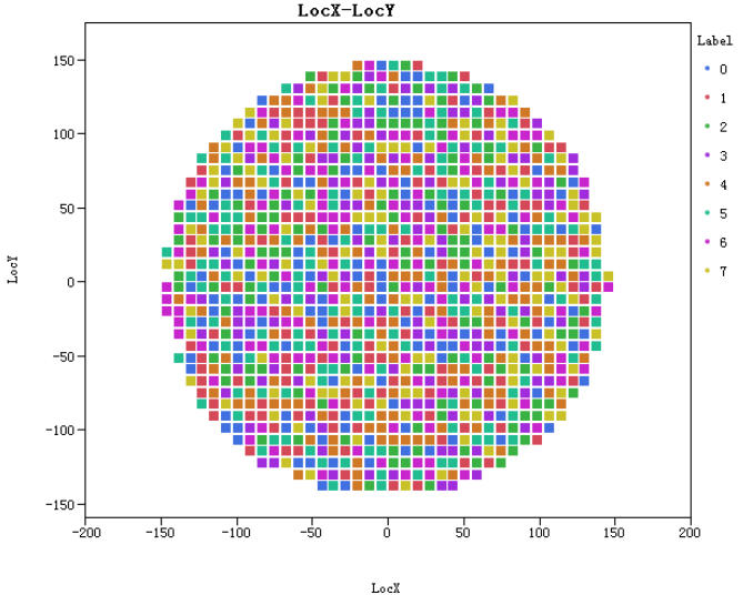
8. The software supports precise positioning map, coordinate data generation, and the database automatically stores data and pictures

Specification

-
Product Features
• Integrated self-made ultra-narrow pulse SMU, minimum pulse to 100ns, maximum current 30A
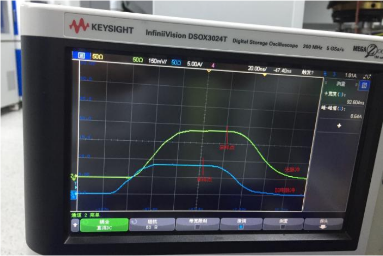
• Integrating sphere synchronous light collection, supporting short pulse LIV test and spectral test
• Development probe, small inductance, supporting narrow pulse high current (minimum pulse 100ns, maximum current 30A) test, four-wire test with double probes, adjustable probe pressure; probe electric slide table control, realizing addressable test and multi-channel test
• Supports wafer position recognition and automatic adjustment
• The test stage uses high thermal conductivity materials, TEC temperature control, and the temperature range can support 25~85°C
• Supports fast spectral testing
• Supports NF uniformity and bad point detection and M2 factor, waist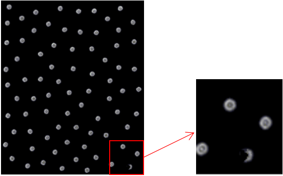
• Supports FF test and divergence angle test

• Software supports precise positioning map, coordinate data generation, and database automatic storage of data and images
-
Parameters
Indicators
Suitable Wafer Sizes
2-inch, 4-inch, and 6-inch
Chip Powering Method
Supports same-side and different-side VCSEL powering
Pulse Current Output
Range 0-30A, accuracy 0.5%rdg±250mA, minimum pulse width 100ns, Duty cycle: ≥1A current <0.1%, <1A current <50%
Voltage Measurement
Range 0-40V, accuracy 0.5%rdg±250mV
Power Test
Using integrating sphere for light collection, range 0-200W, accuracy 0.5% FS±10mW
Wavelength Range
400-1100 nm, other wavelengths support customization
Output Characteristic Curve
(1) LIV characteristic curve (2) Spectral curve
LIV Test Parameters
Ith,V,Ir,SE,Rs,P,PCE,Wavelength,FWHM, etc.
Near-field Test Parameters
Number of light emitting holes, dark defects, consistency, and customizable M2, hole divergence angle, and beam waist test functions
Far-field Test Parameters
Divergence angle (1/e², D86, D50), DIP
Spectral Parameters
λp Peak Wavelength
Addressable Function
Probe electric slide control, realizing addressable testing.
Laser Ranging
Laser ranging is used for chuck and wafer height measurement and leveling, accuracy ≤1um.
Test Stage Temperature Control Range
25~85℃, stability <±1℃
Equipment Dimensions
Excluding signal lights and displays, 1250mm (depth) × 1100mm (width) × 1750mm (height)
Gas Source Requirements
Positive pressure: None
Negative pressure: ≤-80KPa
Power Supply
AC 220V/16A 50Hz
Key words:
Focus on us
Tel
086-27-8990 8766
